PV Nano Cell
  • Home
  • About Us
    • About Us
    • Management Team
    • Board of Directors
    • Advisors
  • Technology
    • Solution
    • Mass Production Applications
    • Digital vs. Screen Printing
    • Sicrys™ Technology
    • R&D Funded Projects >
      • R&D Consortia
      • eurstars™ inkjetPCB
      • Project DigiMan
    • IP & Patents
  • 我们的技术
  • Products
    • Silver Inks >
      • General Purpose
      • Solar, Ceramic & Glass
    • Copper Inks
    • Resistor Inks
    • Gold Ink
    • LIFT Paste
    • Printers
    • Request Quotation
  • 制 品
  • NEWS
    • Press Releases
    • In The News
    • Newsletters
    • Blog
  • Investors
  • Contact Us

Picture
inkjetPCB

Inkjet-based fabrication of multilayer printed circuit boards with embedded printed passive elements. Project duration: 11/2019 – 10/2021

Picture

Picture

Standard PCB industrial manufacturing process
Picture
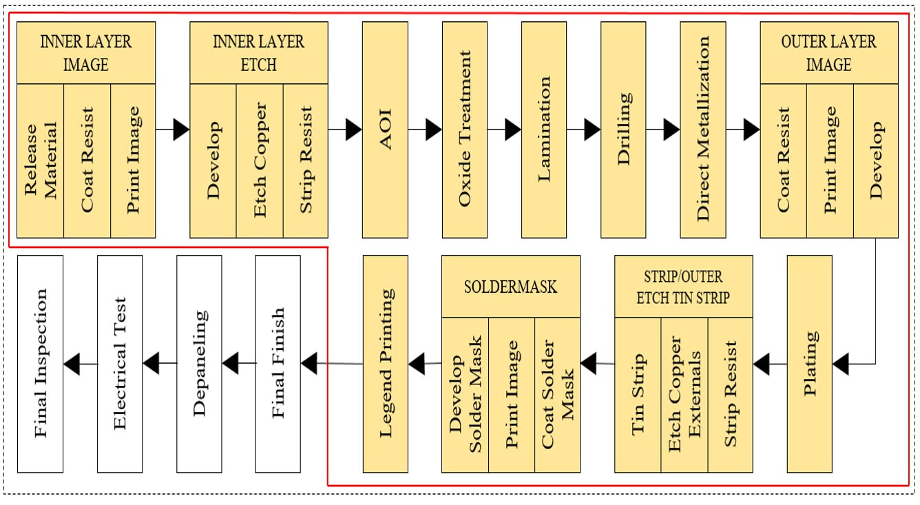
Complex, multi-stage, material intensive, costly, high waste production, environmentally aggressive, SUBTRACTIVE.

inkjetPCB

Picture
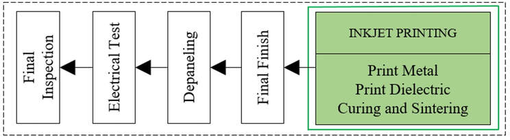
  • Cheaper in terms of processing operations, materials involved, capital investment, workforce employed, waste management.
  • Potentially faster (exploiting high throughput equipment).
  • Increased functionalities: flexibility, passive component embedding, reduced dishomogeneities deriving from plating and etching high or low density patterned areas, etc.
  • The low capex allows high parallelization in order to increase the throughput.
  • Environmentally friendly: no hazardous material employed, additive manufacturing.
  • Drastic reduction of factory floor plan area from 200m2 in the current state-of-the-art process to 60m2 maintaining the same throughput.
  • Digital advantages: product singularization, smart production planning, change on the fly, cheap and fast prototyping.
  • Non-contact process: embedding of PCBs onto 3D objects, printing of fragile substrates.

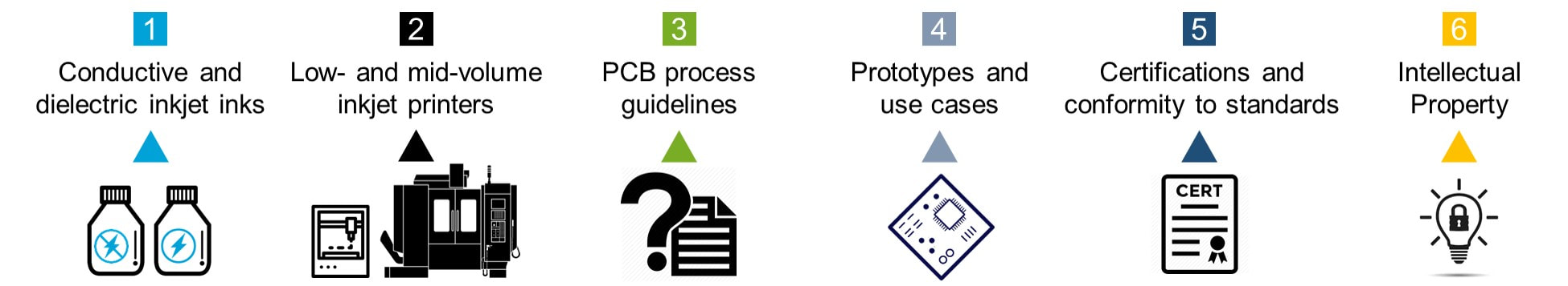
Project objectives and envisaged results

Picture

Partners & Roles

Picture

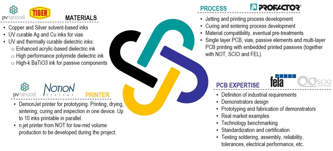
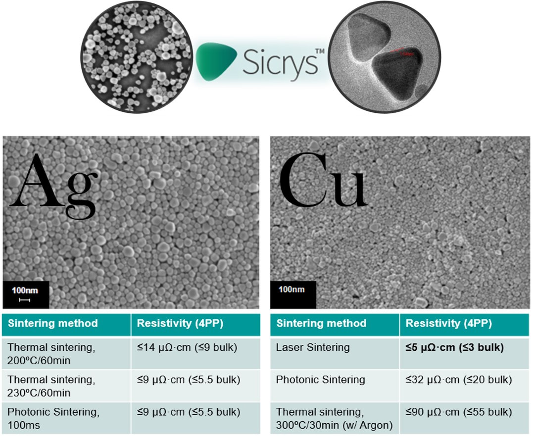
Materials: conductive and dielectric inks

  • Solvent-based metallic inks, from the ink family Sicrys™, as material for conductive lines, contact pads, ground planes and resistors. Copper and Silver inks.
  • UV curable conductive inks under development by PVN for printing high aspect ratio structures, based on silver and copper NPs embedded in a UV curable matrix.
  • UV and thermally curable dielectric inks will be selected and optimized during the project to ensure they meet the expected requirements in terms of printability, electrical and mechanical properties:
                -  Enhanced acrylic-based dielectric ink
                -  High performance polyimide dielectric ink
                -  High-k BaTiO3 ink for passive components
Picture
Picture
Picture

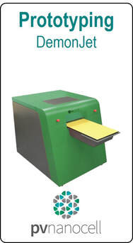
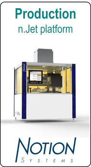
Printers: prototyping and production equipment

  • Large area printing: Standard PCB panel size
  • Multiple materials
  • Multiple printheads
                -  Mixed resolutions capabilities for dielectric and
                   conductive features
                -  Minimum conductive feature size <50µm
  • Throughput enhancement techniques
  • Additional hardware integration
                -  IR drying
                -  UV curing
                -  NIR laser sintering
                -  Vision and inspection system
  • Compatibility with GDS or Gerber files for 3D PCB printing
  • Implementation of missing software features (Embedded components design, Multi thickness lines)
Picture
Picture
Term Of Use - Privacy Policy - General Terms of Sale - Contact Us
  • Home
  • About Us
    • About Us
    • Management Team
    • Board of Directors
    • Advisors
  • Technology
    • Solution
    • Mass Production Applications
    • Digital vs. Screen Printing
    • Sicrys™ Technology
    • R&D Funded Projects >
      • R&D Consortia
      • eurstars™ inkjetPCB
      • Project DigiMan
    • IP & Patents
  • 我们的技术
  • Products
    • Silver Inks >
      • General Purpose
      • Solar, Ceramic & Glass
    • Copper Inks
    • Resistor Inks
    • Gold Ink
    • LIFT Paste
    • Printers
    • Request Quotation
  • 制 品
  • NEWS
    • Press Releases
    • In The News
    • Newsletters
    • Blog
  • Investors
  • Contact Us